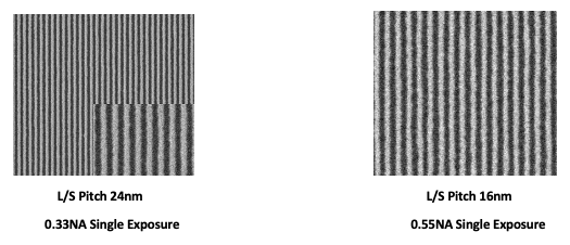
Abstract: The adoption of extreme ultraviolet (EUV) lithography in high-volume manufacturing has enabled continued scaling of semiconductor devices beyond the 7nm logic and 16/14nm DRAM nodes. EUV’s ability to support direct patterning offers significant advantages over multi-patterning techniques, including reduced edge placement error, shorter cycle times, and lower costs.
Despite these benefits, a major challenge remains: achieving high-contrast imaging with sufficient photon delivery to the photoresist. This is critical to meeting requirements for cost efficiency, edge placement accuracy, and low defectivity. While advancements in EUV scanner power, reliability, and numerical aperture have been encouraging, photoresist performance has emerged as a key bottleneck. Current spin-coated resists struggle to meet the stringent demands for sensitivity, resolution, and defectivity at advanced nodes, forcing trade-offs in design flexibility, process complexity, and cost.
This presentation showcases Lam Research’s latest innovations aimed at overcoming these limitations. It introduces novel dry processing techniques that enhance both photoresist application and latent image development, delivering industry-leading performance aligned with advanced technology ground rules. The talk also highlights Lam’s co-optimized solutions for stack design, transfer etch, and post-processing, which collectively address cost and edge placement challenges in advanced patterning. Attendees will gain insight into how Lam’s integrated approach is helping extend the semiconductor roadmap through a comprehensive suite of advanced patterning technologies.

Bio: Rich Wise, PhD leads the patterning technology group in the Lam Research CTO office. Since joining Lam Research in 2014 Dr. Wise has led the introduction of innovative patterning solutions such as dry photoresist supporting the industry migration to EUV and multi-patterning innovations for both logic and memory applications.
Prior to joining Lam Research Rich held the appointment of Distinguished Engineer responsible for plasma based patterning solutions in the IBM Semiconductor Research and Development Center in Fishkill, New York. At IBM Rich led plasma based etch process development for the IBM corporation and both advanced memory and logic technology development alliances.
Rich received his PhD in Chemical Engineering from the University of Houston for his research on inductively coupled non-equilibrium plasmas using numerical simulations and optical spectroscopy techniques. Rich holds over 150 patents in the field of plasma based processing and related semiconductor patterning technologies