March 9, 2020 Photos: 2020 ISSCC MTL CICS Reception February 17, 2020 March 5, 2020 Next-generation nanosystems: A Q & A with Max Shulaker March 2, 2020 Microsystems Annual Research Conference (MARC) highlights students' research, looks to the future of micro & nanotechnology February 24, 2020 Three EECS professors receive fellowships for early stage research Faculty Research Innovation Fellowship recipient Professor Tomas Palacios February 20, 2020 Cryptographic “tag of everything” could protect the supply chain Tiny, battery-free ID chip can authenticate nearly any product to help combat losses to counterfeiting. February 20, 2020 Negar Reiskarimian has been named to an X-Window Consortium Career Development Chair Reiskarimian was one of five EECS faculty members named to career development chairs February 6, 2020 Photos: IAB2020 January 30, 2020 February 6, 2020 Photos: MARC2020 January 28-29, 2020 February 4, 2020 Pablo Jarillo-Herrero wins Wolf Prize for groundbreaking work on twistronics Professor of physics honored alongside Allan MacDonald and Rafi Bistritzer for pioneering research on twisted bilayer graphene. January 23, 2020 Photos: MTL Director's Brunch January 23, 2020 Load More
March 2, 2020 Microsystems Annual Research Conference (MARC) highlights students' research, looks to the future of micro & nanotechnology
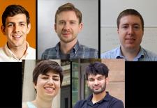
February 24, 2020 Three EECS professors receive fellowships for early stage research Faculty Research Innovation Fellowship recipient Professor Tomas Palacios
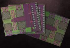
February 20, 2020 Cryptographic “tag of everything” could protect the supply chain Tiny, battery-free ID chip can authenticate nearly any product to help combat losses to counterfeiting.
February 20, 2020 Negar Reiskarimian has been named to an X-Window Consortium Career Development Chair Reiskarimian was one of five EECS faculty members named to career development chairs
February 4, 2020 Pablo Jarillo-Herrero wins Wolf Prize for groundbreaking work on twistronics Professor of physics honored alongside Allan MacDonald and Rafi Bistritzer for pioneering research on twisted bilayer graphene.