
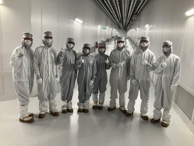
The 2026 Northeast Microelectronics Internship Program (NMIP), organized by the MIT Microsystems Technology Laboratories, brought together 30 exceptional students from leading universities across the Northeast, for an immersive week exploring the rapidly evolving world of semiconductor technology and microelectronics. Held July 13-17, the externship provided undergraduate students with an opportunity to experience the complete microelectronics innovation ecosystem, from academic research laboratories to advanced manufacturing facilities.
Throughout the week, students visited several of the region's premier institutions, including MIT.nano, IBM Research, GlobalFoundries, Rensselaer Polytechnic Institute (RPI), and NY CREATES, where they engaged with researchers, engineers, faculty, graduate students, and industry leaders working at the forefront of semiconductor innovation.
The program began at MIT.nano with an inspiring overview of the microelectronics landscape led by Vladimir Bulović, Director of MIT.nano, and Farhad Varzhegoo, Director of Strategic Initiatives and Partnerships at the Northeast Microelectronics Coalition (NEMC) Hub. Their presentations challenged students to think beyond today's technologies and consider the broader societal impact of tomorrow's innovations.
"What will the next innovation in microelectronics look like, and what should the world of tomorrow focus on?" they asked, encouraging participants to view engineering not only as a technical discipline but also as a means to solve meaningful real-world challenges.
Following the opening session, Professor Farnaz Niroui, the Emmanuel E. Landsman Career Development Chair and Assistant Professor of Electrical Engineering and Computer Science at MIT, organized a series of graduate student research presentations showcasing the breadth of microelectronics research taking place across MIT. The presentations explored topics spanning integrated circuits, nanoelectronics, photonics, quantum technologies, and advanced materials.
After the student research presentations, participants attended an industry panel exploring the transition from academia to careers in microelectronics. Organized and moderated by Susan Feindt, Fellow Emeritus at Analog Devices and Visiting Research Scientist at MIT, the panel featured professionals from Rage Systems, Cadence Design Systems, Analog Devices, and RTX (Raytheon), who shared their career journeys, discussed the differences between research and industry, and offered advice on navigating career opportunities in the semiconductor sector.
“What stood out to me most about our day at MIT was the opportunity to engage deeply with PhD students in this field and understand the kind of opportunities available by pursuing a doctoral program,” said Shanti Visurakapalli, a current undergraduate student at MIT. “I think this experience complemented with the industry panel gave many of us in the program the perspective we needed to weigh future graduate and professional options.”
Throughout the week, participants connected classroom concepts with real-world applications through behind-the-scenes access to some of the nation's most advanced research and manufacturing environments. Students explored MIT's interdisciplinary laboratories, observed High-NA EUV lithography and quantum hardware development at IBM Research, toured GlobalFoundries' state-of-the-art 300 mm semiconductor fabrication facility, learned how groundbreaking academic research transitions into commercial manufacturing at RPI, and gained insight into next-generation semiconductor fabrication at NY CREATES.
"The externship gave me a behind-the-scenes look at the advanced technologies driving the microelectronics industry while allowing me to connect one-on-one with researchers and industry professionals," said Sean Kim, a student at Princeton University. "Learning about emerging research and receiving career advice broadened my perspective on the field and inspired me to pursue a career in microelectronics."
Beyond the technical experiences, the externship emphasized professional development and networking. Students engaged in meaningful conversations with engineers, scientists, faculty members, and graduate researchers who shared their career journeys, offered advice, and discussed the many pathways available within the semiconductor industry. These interactions provided participants with valuable perspectives on careers in research, manufacturing, design, and emerging technologies.
"One of the most rewarding aspects of the externship is seeing students from different universities come together around a shared passion for innovation," said Preetha Kingsview, NMIP Program Administrator. "The friendships they build, the conversations they have with researchers and industry leaders, and the excitement they bring to every visit create an experience that extends far beyond the technical program."
For many students, the experience proved both transformative and inspiring. The opportunity to witness cutting-edge research firsthand while building connections with leaders across academia and industry deepened their understanding of the semiconductor ecosystem and reinforced the critical role microelectronics plays in addressing global challenges.
"For more than half a century, microelectronics has transformed the world, but I believe its most exciting chapter is only just beginning," said Tomás Palacios, Clarence J. LeBel Professor of Electrical Engineering and Computer Science at MIT, and Faculty Director of the NMIP Program. "From AI and quantum computing to sustainable energy and advanced manufacturing, nearly every technological revolution of the coming decades will be built on advances in semiconductor technology. Today's undergraduate students will become tomorrow's innovators, entrepreneurs, and industry leaders, and programs like the NMIP Externship help inspire and prepare them to shape that future."
By bringing together leading universities, research institutions, and industry partners, the program provides students with a comprehensive view of the semiconductor ecosystem while helping build the highly skilled workforce needed to sustain U.S. leadership in microelectronics.
The 2026 externship demonstrated the power of connecting education, research, and industry. Through a week of laboratory tours and technical presentations, it gave students a firsthand view of how scientific discovery becomes technological innovation - and inspired many to become part of the future of microelectronics themselves.
Acknowledgements.
The organizers gratefully acknowledge the generous support of the Microelectronics Commons Northeast Microelectronics Coalition (NEMC) Hub and the Microelectronics Commons Northeast Regional Defense Technology Hub (NordTech), whose sponsorship made the 2026 NMIP Externship possible. Additional support was provided by the MIT Microsystems Technology Laboratories (MTL), the MIT Institute for Soldier Nanotechnologies (ISN), and the Semiconductor University Research Program for Superior Energy-Efficient Materials and Devices (SUPREME) Center, part of the SRC JUMP 2.0 program. The organizers also extend their sincere appreciation to the many participating companies, universities, and research institutions—including MIT.nano, IBM Research, GlobalFoundries, Rensselaer Polytechnic Institute (RPI), NY CREATES, Rage Systems, Cadence Design Systems, Analog Devices, and RTX—as well as to the faculty, students, engineers, and staff whose time, expertise, and enthusiasm created an exceptional learning experience for the next generation of microelectronics innovators.