1960
- Semiconductor Electronics Education Committee (SEEC) established.
1968
- Integrated Microelectronics Laboratory (“Microlab”) opens in Building 13.
1977
- Submicron Structures Laboratory (SSL) established in Building 13, rechristened NanoStructures Laboratory (NSL) in 1994.
1978
- First offering of Introduction to VLSI Systems, a multi-project chip design course.
1979
- MIT VLSI Seminar launched (renamed MTL Seminar in 2007).
- Dimitri Antoniadis appointed as first director.
1980
- MIT announces plans for establishing MTL (originally termed LSI Fabrication Facility).
1982
- Weekly lunch meeting (“microlunch”) of microsystems faculty starts; it continues to this day
- Microsystems Industrial Group launched.
1984
- MTL opens, reporting to Department of Electrical Engineering and Computer Science; initial set of labs:
1986
- Building 39 dedicated as Gordon Stanley Brown Building.
1989
- Full CMOS process qualification of ICL achieved.
- CAFE (Computer Aided Fabrication Environment) software system developed.
- Richard Adler appointed as MTL co-director with Dimitri Antoniadis.
1990
- Process Technology Committee established.
- Rafael Reif appointed as MTL director.
1991
- Process Technology Committee established.
1994
- MTL and NSL spawn Space Nanotechnology Laboratory in Building 37.
1995
- MTL reporting moves to School of Engineering.
1998
- Center for Integrated Circuits and Systems established.
1999
- Bldg. 13 Microlab moves to Building 39 and becomes Exploratory Materials Laboratory (EML).
- Martin Schmidt appointed as MTL director.
2000
- Class 1 Committee report on MTL fab operations issued.
2001
- 4” to 6” wafer diameter conversion completed.
2002
- Microsystems Affiliate Program for industrial users established, renamed Fabrication Facilities Access Program in 2004.
2003
- CORAL fab management software system deployed (replacing CAFE).
2006
- Anantha Chandrakasan appointed as MTL director.
2009
- MUMMS/Cost Recovery deployed enhancing MTL's lab management software suite.
2011
- Vladimir Bulović appointed as MTL director.
2012
- Electron Beam Lithography Facility (EBL) established in Building 24; managed jointly with the Research Laboratory of Electronics (RLE).
2013
- Jesús del Alamo appointed as MTL director.
2014
- MIT.nano, a new 200,000-square-foot center for nanoscience and nanotechnology, announced.
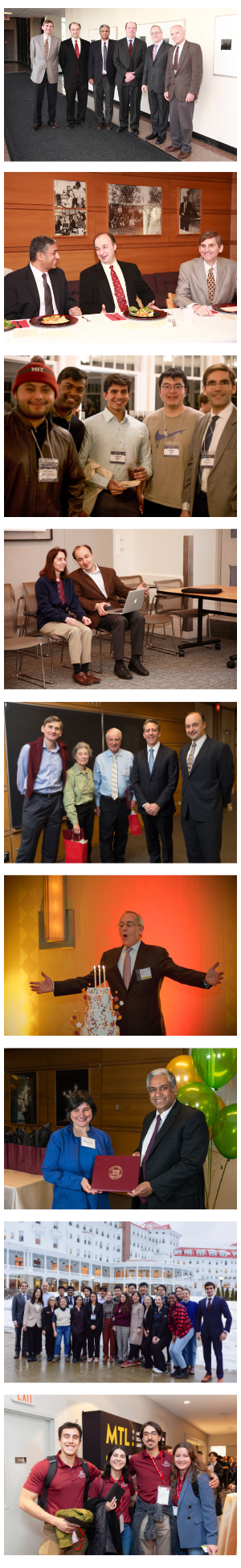
- MTL 30 year celebration takes place.
2018
- MIT.Nano opens, MTL becomes "fabless."
2019
- Hae-Seung (Harry) Lee appointed as MTL director.
2022
- Tomás Palacios appointed as MTL director.
- CHIPS and Science Act
2023
- MTL becomes founding member of the Northeast Microelectronics Coalition (NEMC)
2024